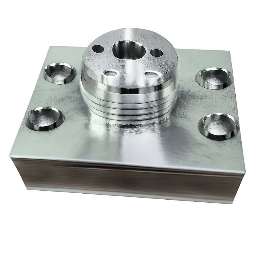
Semiconductor Equipment Components
Ultra-clean precision machining for wafer equipment core components, meeting Class 1000 cleanliness requirements
Why Semiconductor Parts Are Hard
Semiconductor equipment does not accept "close enough." Wafer transfer mechanism positioning accuracy directly impacts yield; chamber part outgassing affects vacuum level; surface roughness affects particle generation. One detail overlooked, and the entire production line suffers.
Our Approach
Bisite has served semiconductor equipment customers since 2018, currently supplying 6 domestic semiconductor equipment manufacturers in volume. We have the most experience with precision machining of 316L stainless steel and 6061 aluminum — electropolishing and passivation are done in-house, no outsourcing required.
Cleanliness control is not just a final wipe-down — it is managed end-to-end from machining environment through packaging and shipping, with final cleaning and inspection under Class 1000 cleanroom conditions.
Quality Traceability
Every part has a unique batch number — from raw material incoming inspection through machining parameters, inspection records, and shipping reports, fully traceable. We have produced hundreds of FAI first article reports and PPAP documents — the process is second nature.